9. FMC side
9.1. Two HPC
9.1.1. Available signals
Many lpGBT signals are available across the two FMC HPC connectors (J1 and J2). This allows a Front-End board or an FPGA evaluation kit to monitor/drive
these signals. Almost all the e-links and Phase Shifter clocks (ECLK0 and PSCLK1 on SMA) are available in both HPC.
The HPC-elinks pin connectivity is listed in the Section 13.
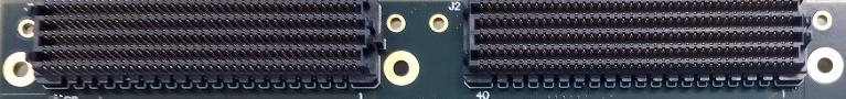
Fig. 9.1 VLDB+ HPC connectors
9.1.2. Matched lengths
In the VLDB+, all the EPRX and 7 ECLK have been length matched for a tolerance of 4 mm. However, as the VLDB+ is mainly conceived to work together with an Evaluation Kit FPGA as the VC707, the length of these signals, that are going from the HPC connectors to the FPGA on the Evaluation Kit, has also been taken into account.
As the average length of EPRX signals going from the VC707 HPC1 to the FPGA is around 32 mm shorter than the ones going from the VC707 HPC2 to the FPGA,
in the VLDB+, the signal length of each EPRX going to the HPC1 (J1) is 32 mm higher than the ones going to the HPC2 (J2).
The same thing occurs with the 7 ECLK signals which are length matched. From those 7, there are 3 going to the HPC1 (J1) and in consequence,
its signal lengths are ~32mm higher than the other 4 ones going to the HPC2 (J2).
No length matching has been applied for the EPTX though.
All the information about the signal lengths of the E-link signals is listed in the Section 13.
9.2. Protection switches
Warning
VLDB+ V1 known issues: Section 14.1.4.
The VLDB+ also makes most of the lpGBT’s slow control signals available through one of the FMC HPC connectors (HPC2). However, this
has to be performed with care as the lpGBT only handles 1V2 LVCMOS. For this purpose, 4 protection switches of 8 pins each
(SW1, SW2, SW3, SW4) have been inserted between the FMC and the lpGBT as a safety feature. Refer to the Section 13.7 for more information.
These switches, however, only protects the lpGBT when properly used and still require a careful configuration of the electronics connected on the FMCs.
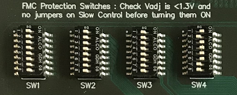
Fig. 9.2 VLDB+ Protection_switches
To have access to those lpGBT signals through the Evaluation Kit FPGA, you have to follow the next steps.
- Set all the protection switches to OFF.
- Configure the VADJ of the FPGA evaluation kit to 1.2 V (or the front-end board). A VADJ > 1.3 V shall turn on the LED1 into RED. For the KCU105, VCU108, VCU118 and ZCU102 Evaluation Kits, VADJ will be set automatically to 1.2 V. Refer to Section 9.3.
- Configure the IOs from the FPGA or the front-end board with the LVCMOS12 IOstandard.
- On the FPGA/Front-End board, configure each IO direction according to the lpGBT configuration. Check both directions and levels on the switches pins.
- Configure the lpGBT with the right configuration (in particular for the IO directions). Check on the pins of the switches as well.
- Remove ALL JUMPERS from the GPIO/ADC slow control area.
Once all the steps 1 to 6 have been performed, carefully turn on the required switches to have access to all the lpGBT’s slow control signals.
In the case where VADJ is higher than 1.3 V, the red LED1 will be lit automatically when SW10 is on. If this happens, the FPGA Evaluation Kit or front-end has to
be turned off immediately.
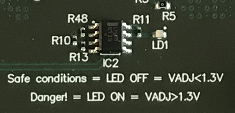
Fig. 9.3 VLDB+ Warning LED
Warning
If the LED1 is lit when the VLDB+ is on, it means that VADJ > 1.3 V. If the protection switches are enabled when this happens, the lpGBT is receiving from
the Slow control pins more voltage than the recommended. Turn off immediately the front-end connected to the VLDB+ if this happens.
9.3. EEPROM
The VLDB+ houses an EEPROM IC3 close to the HPC connectors to comply with the VITA57.1 standard. On its memory, there are almost 256 8-bit values
that describes the voltage levels of the FMC HPC system. For more information refer to the IPMI FRU and
ANSI VITA57.1 .pdfs. When connecting the VLDB+ to a KCU105, VC108, VC118 or ZCU102 evaluation kit, when turned on, these will
read the IC3 EEPROM to set the VADJ voltage level to the defined value on its memory. This will be in our case VADJ = 1.2 V.
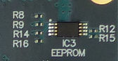
Fig. 9.4 VLDB+ EEPROM
Note
The EEPROM is programmed with specific memory values to work with these evaluation kit FPGAs. If this information is erased, the FMC connectivity with them will not work as VADJ will be set to 0 V.
Note
The KCU105 evaluation kit have troubles to set VADJ when detecting the HPC2 through the HPC2_PRSNTM2C_L signal. In the VLDB+, the 0 Ω resistor R4 is
not populated to remove the HPC2_PRSNTM2C_L signal and avoid problems when connecting the VLDB+.