6. VLDB+ switches
6.1. lpGBT Modes
The lpGBT chip has many modes of operation that can or must be set through configuration pins (Configuration pins).
On the VLDB+, those pins are accessible through 3 different switches. The mode of operation (TX, RX, TRX, FEC), the programming mode
(SC or I2C), the I2C address (ADDR[3:0]), the locking mode (CDR or External) and the testing modes (disable Power On Reset
and force a lpGBT’s state through Stateoverride) can be simply set and unset with these switches. Switch it to the right to enable the specific mode.
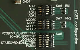
Fig. 6.1 lpGBT modes in the VLDB+ V2
Note
When the PiGBT is connected to the VLDB+, the control of the MODE[3:0] is done through the PiGBT web interface only.
This means that changes made through the switches will have no effect.
Note
In the VLDB+ V2, some of the lpGBT V0 and V1 configuration pins are shared by the same switch SW8. In the silkscreen, look at the left side of the slash
when having an lpGBT V0 housed and at the right side of the slash when having an lpGBT V1 to well configure your lpGBT. The LOCKMODE and
the PORDIS pins did not change between lpGBT versions.
6.2. I2C pull-ups
In addition, you can add I2C pull-up resistors on all the available I2C lines (master and slave) through the SW5.
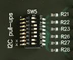
Fig. 6.2 I2C pull-ups on SW5
Note
Pins 7 and 8 of SW5 are left unconnected. Pull-ups go from pin 1 to pin 6. Refer to the Section 13.9.