8. lpGBT’s slow control
8.1. RPI and Dongle connector
Warning
VLDB+ V2 known issues: Section 14.2.2.
The lpGBT has to be configured to properly start up (its blank configuration does not allow it to lock on serial frames). The simplest way to do it is by using the lpGBT I2C controller. To do so, we provide a control toolkit made of:
- A
Raspberry PI 4(featuring the PiGBT control software). - An ad-hoc PI translator board.
- A 10-pin cable to communicate with the lpGBT through the
J13connector.
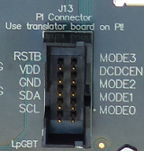
Fig. 8.1 Raspberry PI and Dongle connector
We can also set the lpGBT’s mode of operation, reset the lpGBT and reset both FEASTMPs DC/DC through it. Note as well that J13 is pin compatible
with the CERN’s Dongle (provided that it is configured to deliver/receive 1V2 instead of the traditional 1V5 used by the GBTx).
With the Dongle, only I2C communication is available (SDA and SCL). No lpGBT software is provided for the Dongle though.
Note
The J10 connector has two polarization slots. Use the one on the left to connect the Dongle cable (only 8 pins used) and the one in the right to connect the Raspberry Pi one (all the pins used).
Note
When connecting the Dongle, the RSTB and MODE3 pins which are left unconnected slightly bend. You might not be able to put a PI cable on the connector afterwards if these
mentioned pins are bent. Please, unbend them with care to reconnect a PI cable.
8.2. ADC
The lpGBT has, in total, 8 independent ADCs. All the ADCs are both connected to FMC HPC and to specific jumpers on the VLDB+,
each of them allowing to perform a different conversion, as described below (except ADC7 which is only connected to the FMC):
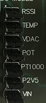
Fig. 8.2 lpGBT’s ADC in the VLDB+
ADC0- Adapted VTRx+ RSSI.ADC1– VTRx+ temperature sensor (10kΩ thermistor VTRX+ V10, 1kΩ pre-prod VTRx+).ADC2– lpGBT VDAC.ADC3– VLDB+ potentiometer.ADC4– VLDB+ temperature sensor (PT1000 sensor)ADC5– Adapted FEASTMP 2.5V output.ADC6– Adapted VLDB+ voltage input.
Take into account that many of the features have been adapted to 1 V range as the maximum output voltage level. In case of using the lpGBT current DAC, ensure what is the resistance of the output to avoid exceeding 1 V (i.e VTRx+ version for temperature sensor).
To have access to a feature, just connect the required jumper. Note that the concurrent use of the FMC and the jumper is forbidden. For each ADC, a protection switch, OFF by default (Section 9.2) is implemented between the FMC HPC2 and the specific ADC to avoid any conflict.
Warning
Keeping the ADC protection switches off is mandatory before inserting any jumper. It is the user’s responsibility to handle them properly.
8.2.1. VTRx+ RSSI jumper
In the VLDB+ V1, before using the ADC0 to read the adapted value of the VTRx+ RSSI, another jumper must be put on the W2. The jumper position depends on the optical receiver
used on the VTRx+, as the lpGBTIA (1.2 V) and the GBTIA (2.5 V) work with different voltage levels. The VTRx+ delivered with any VLDB+ work with the
GBTIA optical receiver, thus, a jumper has to be put on the left side (pull-up to 2.5 V) to read the RSSI adapted value through the ADC0.

Fig. 8.3 Jumper to be put on W2 for the VTRx+ RSSI reading.
Note
The VLDB+ V2 does not feature any RSSI jumper. There, the VTRx+ RSSI is pulled-up to 2.5V as the pre-production version of the VTRx+ uses the GBTIA optical receiver.
8.3. GPIO
The lpGBT has, in total, 16 independent GPIOs. All the GPIOs are connected to the FMC HPC (for Front-End or FPGA control/monitoring).
In addition, 6 GPIOs out of 16 are connected to specific jumpers on the VLDB+, each of them allowing to perform a different action,
as described below (GPIO[6:15] are connected only to the FMC):
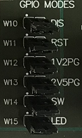
Fig. 8.4 lpGBT’s GPIO in the VLDB+
GPIO0– Disable VTRx+. GPIO used only as an output.GPIO1– Reset VTRx+. GPIO used only as an output.GPIO2– FEASTMP1.2 power good. GPIO used only as an input.GPIO3– Adapted FEASTMP2.5 power good. GPIO used only as an input.GPIO4– VLDB+ switch. GPIO used only as an input.GPIO5– VLDB+ LED. GPIO used only as an output.
To have access to a feature, just connect the required jumper. As for the ADCs, note that the concurrent use of the FMC and the jumper is forbidden. For each GPIO, a protection switch, OFF by default (Section 9.2) is implemented between the FMC HPC2 and the specific GPIO to avoid any conflict.
Warning
Keeping the GPIO protection switches off is mandatory before inserting any jumper. It is the user’s responsibility to handle them properly.
Note
If SW9 has glue around it is because this specific VLDB+ batch had assembly issues with that switch. Please refer to Section 14.2.3 for more information.
8.4. DAC
The lpGBT features 1 DAC. It is connected to the FMC HPC and it can also be connected to the ADC2 with the required jumper (W5) as shown in the
Section 8.2. There is a third feature where you can plug a multimeter probe on the W1 (VDAC on the left pin, GND on the right pin)
to monitor the DAC output voltage.
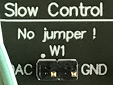
Fig. 8.5 DAC output to monitor
Warning
Do not connect any jumper on the W1 pins! The W1 pins are made to connect a multimeter probe!
8.5. External Control
The lpGBT has three differential pairs called EDOUTECP/N, EDINECP/N and ECLK28P/N that can be used for several purposes. In the VLDB+,
we have connected those pairs to one mini HDMI connector, J12. This way, it is possible for the lpGBT to communicate
with the SCA housed on a former VLDB by connecting both boards through an mDHMI-mHDMI cable (VLDB+ J12 to VLDB J32).
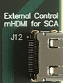
Fig. 8.6 lpGBT’s external control in the VLDB+
The lpGBT has three differential pairs called EDOUTECP/N,
8.5.1. LpGBT-SCA communication guide
Take the following steps to be able to communicate with an SCA through your LpGBT EC channel (lpGBT V1):
- Interconnect the VLDB+ and the VLDB through a mini-HDMI to miniHDMI cable.
- Power-on your VLDB with the FEASTMP1V5 to power the SCA housed on it.
- Follow the quickstart guide in Section 2 and configure your LpGBT to reach Ready state over the optical fiber.
- Then program your LpGBT with:
- [0x0cf] EPRXEcControl EPRXECEnable = 1’b1 (Enables the EC channel input) and EPRXECTrackMode = 1’b0 (Continuous phase tracking)
- [0x0ec] EPRXEcChnCntr EPRXECTerm = 1’b1 (Enables the 100 Ohm termination for EC channel)
- [0x0ac] EPTXEcChnCntr EPTXEcEnable = 1’b1 (Enables the EC channel output) and EPTXEcDriveStrength[2:0] = 3’d7 (4.0mA)
- [0x0a6] EPCLK28ChnCntrH EPCLK28DriveStrength[2:0] = 3’d7 (4.0mA) and EPCLK28Freq[2:0] = 3’d1 (40MHz)
- Execute from your back-end the necessary commands to send through the EC channel the HDLC commands to the SCA.