10. SMA connectors
Warning
VLDB+ V1 known issues: Section 14.1.3, Section 14.1.1.
The VLDB+ features 6 SMA connectors.
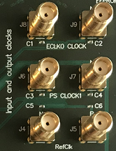
Fig. 10.1 VLDB+ SMA connector
- The first SMA pair (
J8andJ9) corresponds to the lpGBT’s Elink output clock 0ECLK[0]P/N. - The second SMA pair (
J6andJ7) corresponds to the lpGBT’s Phase Shifter output clock 1PSCLK[1]P/N. - Finally, the last pair (
J4andJ5) corresponds to the lpGBT’s Reference input clockREFCLKP/Nwhich is needed to make the lpGBT lock inExternal lockmodeandSimplex Txmode.